The Brave New World of Wafer-Scale Processors: TSMC’s Innovative Leap
Imagine a world where your computer’s brain is not just faster and more power-efficient, but also massively more complex, able to tackle tasks and computations that seem near-impossible today. This isn’t a snippet from a sci-fi novel; it’s the reality TSMC is sculpting with its groundbreaking System-on-Wafer integration technology, known as InFO-SoW, which debuted in 2020. As it stands, trailblazers like Cerebras and Tesla have already hitched their wagons to this star, developing wafer-scale processor designs that are nothing short of revolutionary. Despite the Herculean challenges inherent in crafting these wafer-scale behemoths, TSMC is betting big on their future, envisioning a surge in adoption fueled by the relentless demands of AI and high-performance computing (HPC).
Enter Tesla Dojo: A Glimpse into the Future
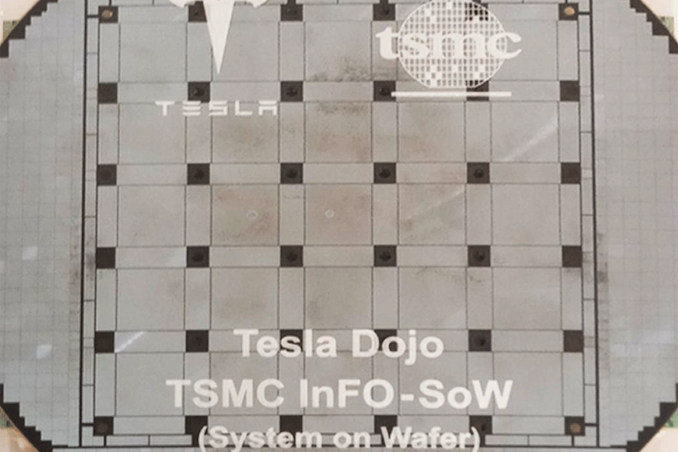
Let’s talk about Tesla’s Dojo for a second—this beastly wafer-scale processor, now in mass production, is TSMC’s poster child for InFO-SoW’s capabilities. Unlike the run-of-the-mill system-in-packages (SiPs) we’re used to, Dojo sets a new benchmark with its low-latency, high-bandwidth communications between cores, jaw-dropping performance and bandwidth density, and energy-efficient delivery networks. Yet, for all its prowess, the reliance on on-chip memory and the necessity to use a single fabrication tech over the whole wafer present new puzzles to solve, especially for NextGen AI workloads.
A Step Towards the Future: TSMC’s Innovative Fusion
Not resting on its laurels, TSMC is already crafting the next chapter in the system-on-wafer saga. By marrying two of its pioneering packaging technologies—InFO-SoW and System on Integrated Chips (SoIC)—through its innovative Chip-on-Wafer (CoW) method, TSMC is setting the stage for even more complex processor designs. Slated for mass production in 2027, this next-gen platform aims to seamlessly integrate memory (like the HBM4 with its 2048-bit interface) atop a wafer-scale processor, bridging the gap between logic power and data storage capacity. This leap isn’t just about keeping pace; it’s about setting the pace, crafting the future of computing with an eye towards ever-greater integration and efficiency.
Raising the Bar: Memory Meets Logic
The fusion of wafer-scale processors with cutting-edge memory technology like the HBM4 isn’t just a technical achievement; it’s a harbinger of the leaps in logic and memory integration we can expect going forward. As Kevin Zhang, TSMC’s Vice President of Business Development, puts it, “SoW is no longer fiction.” It’s here, transforming the dreams of yesterday into the tangible breakthroughs of today and tomorrow. By pushing the boundaries of wafer-level integration, TSMC isn’t just offering a new product; it’s charting a course for the future of computation, especially in AI and supercomputing clusters, heralding a new era of energy-efficient, high-capacity computing.
In a nutshell, TSMC’s innovative foray into system-on-wafer and beyond isn’t merely about scaling up; it’s about imagining and then creating the computing paradigms of the future. As the lines between the physically possible and the imaginatively conceivable continue to blur, one thing is clear: we’re not just witnessing the evolution of technology; we’re actively participating in a revolution.


