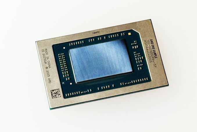
Back at Computex 2024, AMD unveiled their highly anticipated Zen 5 CPU microarchitecture during AMD CEO Dr. Lisa Su’s opening keynote. AMD announced not one but two new client platforms that will utilize the latest Zen 5 cores. This includes AMD’s latest AI PC-focused chip family for the laptop market, the Ryzen AI 300 series. In comparison, the Ryzen 9000 series caters to the desktop market, which uses the preexisting AM5 platform.
Built around the new Zen 5 CPU microarchitecture with some fundamental improvements to both graphics and AI performance, the Ryzen AI 300 series, code-named Strix Point, is set to deliver improvements in several areas. The Ryzen AI 300 series looks set to add another footnote in the march towards the AI PC with its mobile SoC featuring a new XDNA 2 NPU, from which AMD promises 50 TOPS of performance. AMD has also upgraded the integrated graphics with the RDNA 3.5, which is designed to replace the last generation of RDNA 3 mobile graphics, for better performance in games than we’ve seen before.
Further to this, during AMD’s recent Tech Day last week, AMD disclosed some of the technical details regarding Zen 5, which also covers a number of key elements under the hood on both the Ryzen AI 300 and the Ryzen 9000 series. On paper, the Zen 5 architecture looks quite a big step up compared to Zen 4, with the key component driving Zen 5 forward through higher instructions per cycle than its predecessor, which is something AMD has managed to do consistently from Zen to Zen 2, Zen 3, Zen 4, and now Zen 5.
AMD Zen 5 Microarchitecture: 16% Better IPC Than Zen 4
Both the AMD Ryzen AI 300 series for mobile and the Ryzen 9000 series for desktops are powered by AMD’s latest Zen 5 architecture, which brings a host of improvements in performance and efficiency. Perhaps the biggest improvement within their mobile lineup is the integration of the XDNA 2 NPU, which is designed to make use of the Microsoft Copilot+ AI software. These new mobile processors via the NPU can deliver up to 50 TOPS of AI performance, making them a significant upgrade in AMD’s mobile chip lineup.
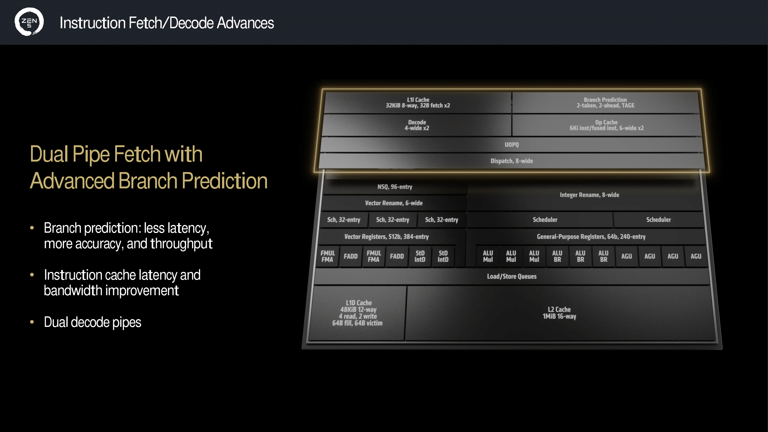
The key features under the hood of the Zen 5 microarchitecture include a dual-pipe fetch, which is coupled with what AMD is calling advanced branch prediction. This is designed to reduce the latency and increase the accuracy and throughput. Enhanced instruction cache latency and bandwidth optimizations further the flow of data and the speed of the data processing without sacrificing accuracy.
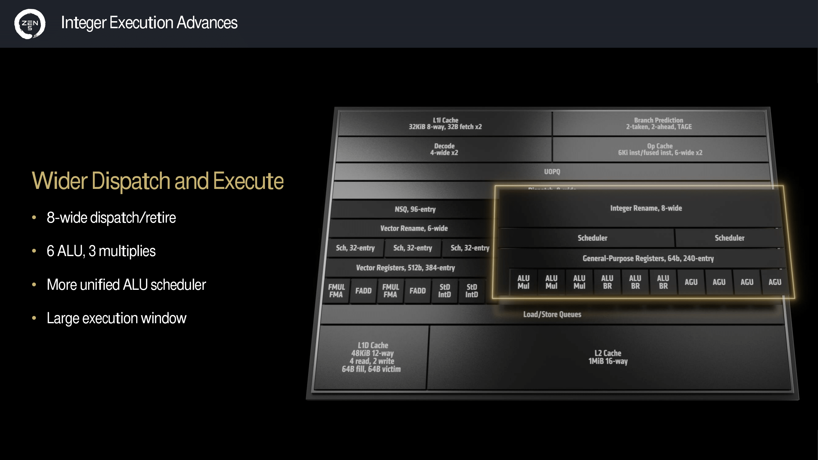
The Zen 5 integer execution capabilities have been upgraded over Zen 4, with Zen 5 featuring an 8-wide dispatch/retire system. Part of the overhaul under the hood for Zen 5 includes six Arithmetic Logic Units (ALUs) and three multipliers, which are controlled through an ALU scheduler, and AMD is claiming Zen 5 uses a larger execution window. These improvements should theoretically be better with more complex computational workloads.
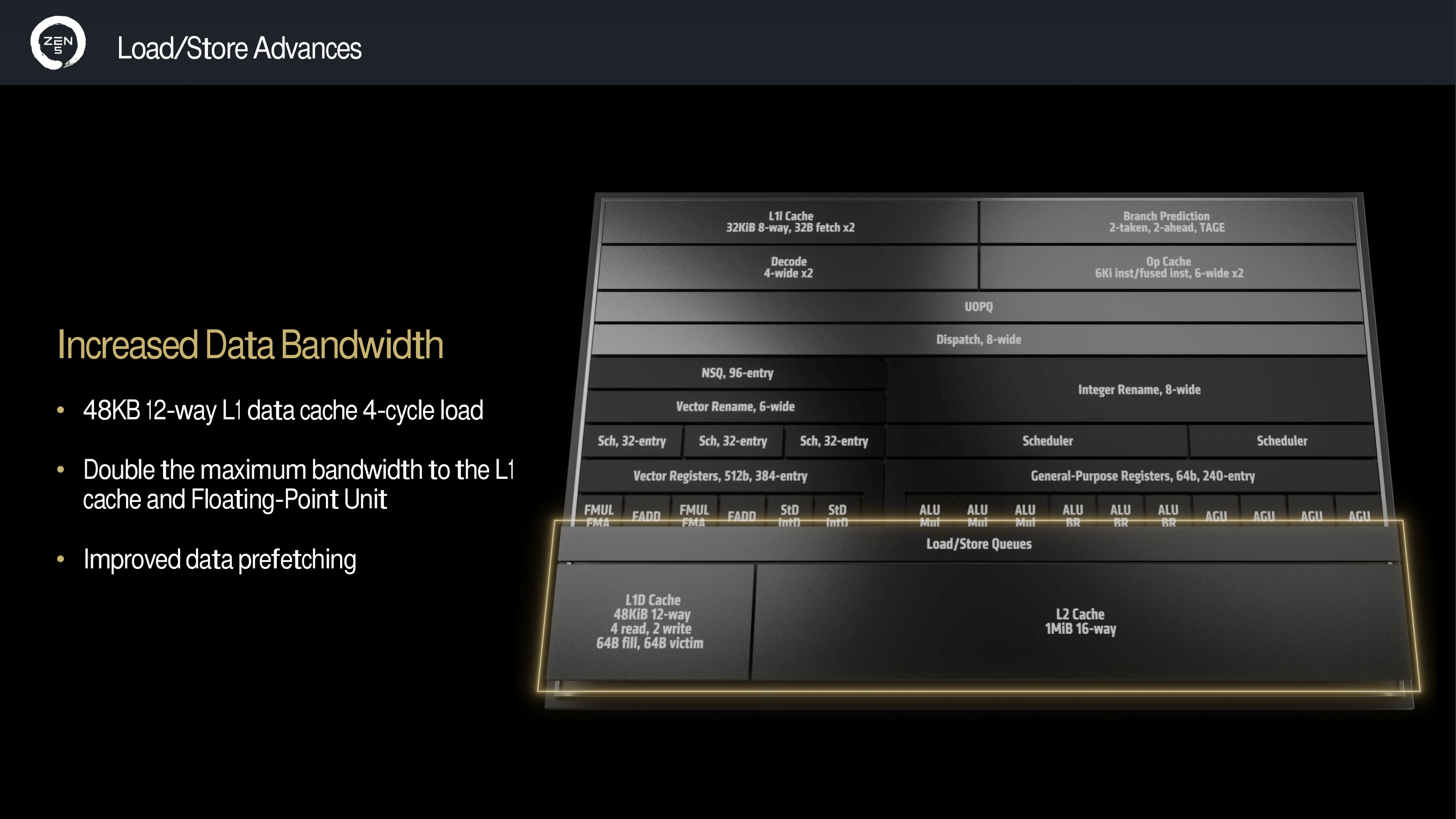
Other key enhancements that Zen 5 comes with include more data bandwidth than Zen 4, with a 48 KB 12-way L1 data cache that can cater to a 4-cycle load. AMD has doubled the maximum bandwidth available to the L1 cache, and the Floating-Point Unit has been doubled over Zen 4. AMD also claims it has improved the data prefetcher, which ensures faster and more reliable data access and processing.
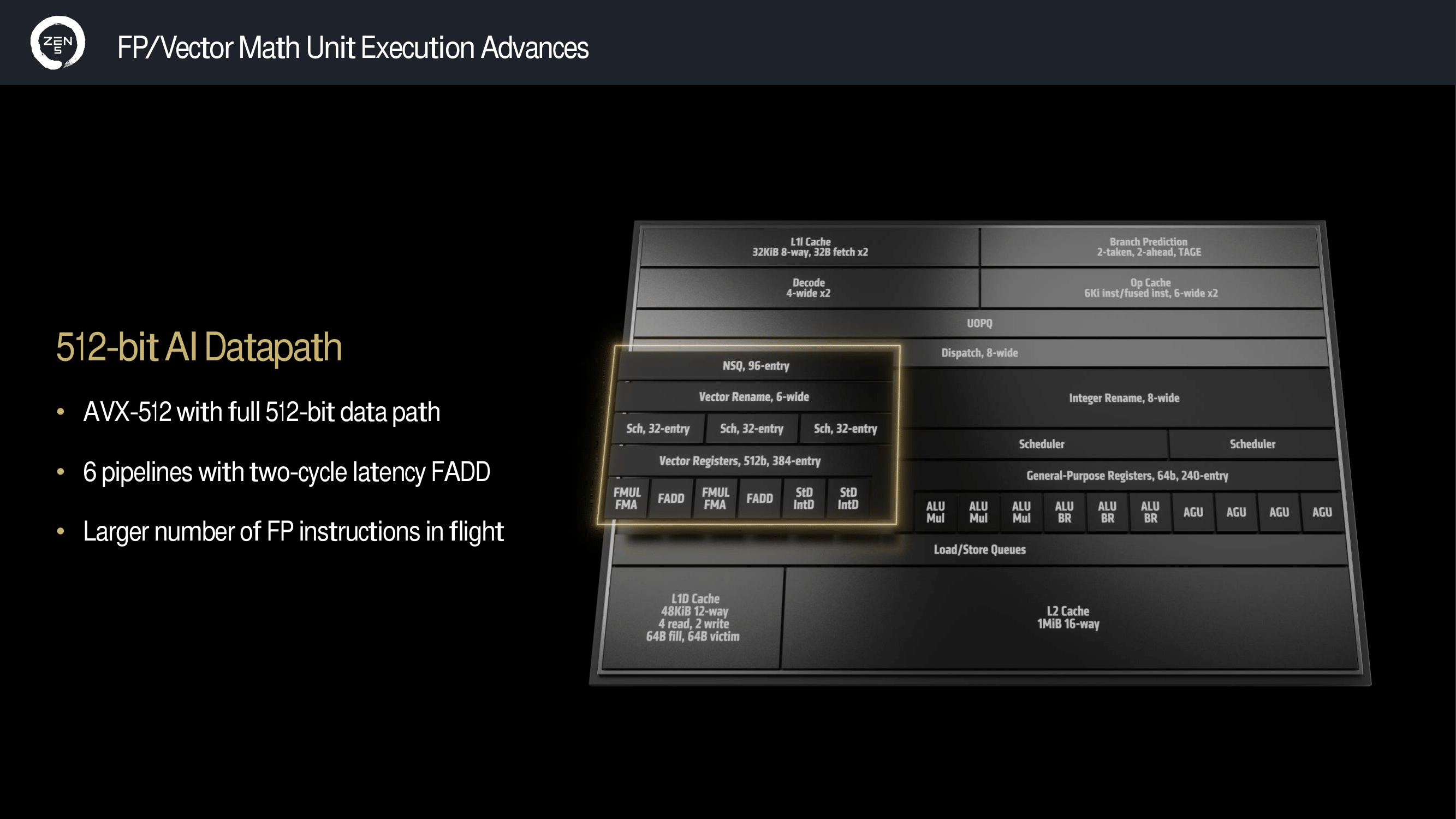
Zen 5 also introduces a full 512-bit AI datapath, which uses AVX-512 with the full 512-bit data path and six pipelines with two-cycle latency FADD. Although Zen 4 can support AVX-512 instructions, it uses two 256-bit data paths that work in tandem with each other, with the term ‘double pumping’ being the most widely used term for it. Zen 5 now has a full AVX-512 data path, which is a welcomed improvement.
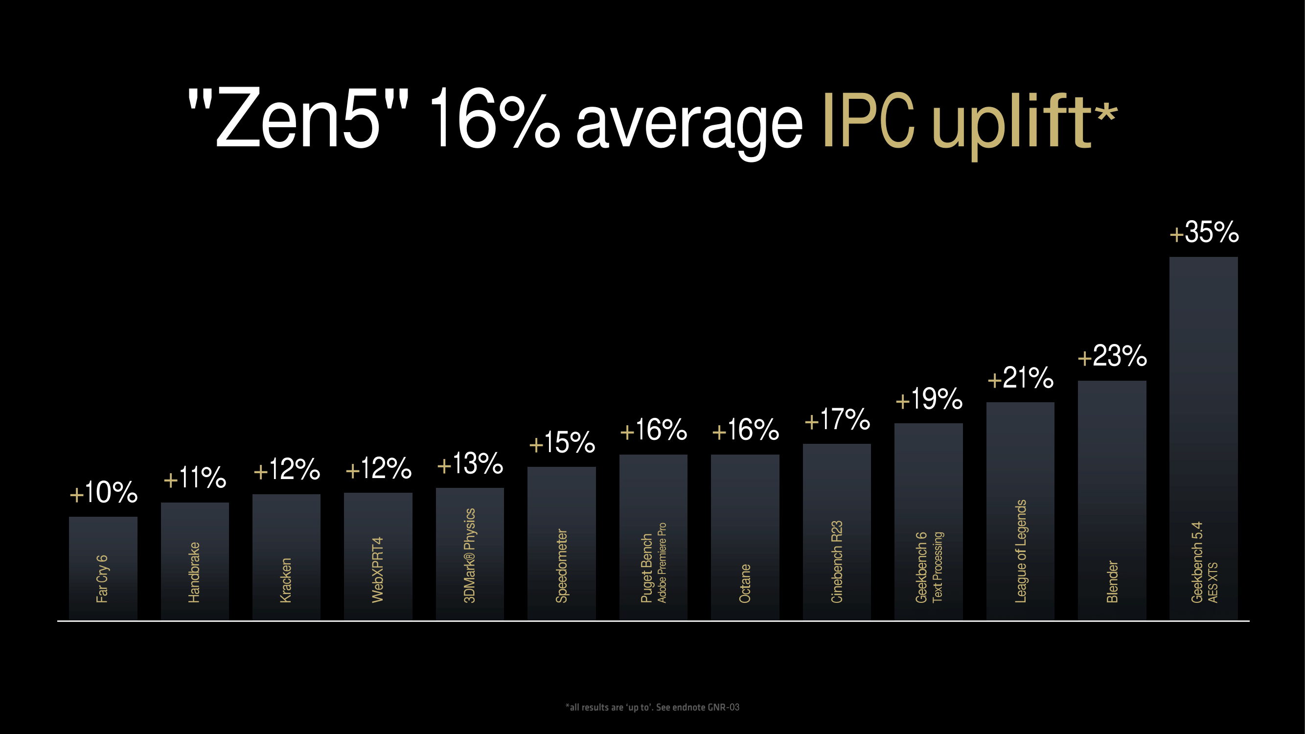
Looking at what AMD is claiming regarding the IPC uplift for Zen 5, AMD claims an average improvement of 16% over Zen 4. AMD has, of course, provided in-house figures, which show across-the-board improvements in various benchmarks. This includes a 10% uptick in Far Cry 6 to 15% in Speedometer and an even bigger uplift of 21% in League of Legends. AMD’s biggest claim is a large 35% improvement in Geekbench 5.4 AES-XTS. That’s an impressive uplift in performance, although the Geekbench 5 AES XTS test utilizes VAES+ and AVX10/512, which for processors that support these instructions as Zen 5 does can be advantageous.
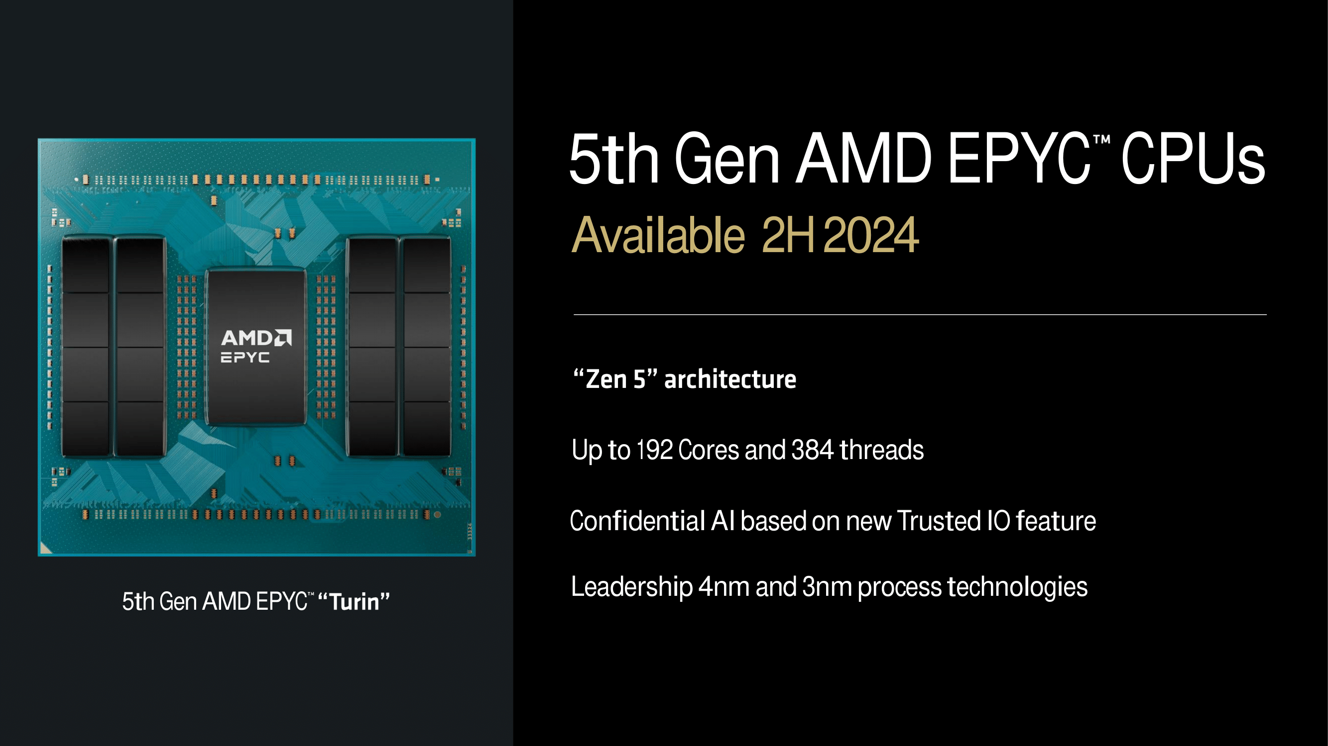
As we’ve seen through previous iterations of their Zen microarchitecture, AMD is making Zen 5 available across the entire product family. The full-fat Zen 5 cores are made on TSMC’s 4nm anode, while the more compact and more power-efficient Zen 5c cores are made on TSMC’s 3nm process technology. AMD’s upcoming 5th generation EPYC CPUs, codenamed ‘Turin,’ are expected to launch sometime in the second half of 2024, which leverage up to a whopping 192 Zen 5 cores. AMD previously announced that 5th Gen EPYC would be coming in 2024 back in June 2022 during their Financial Analysts Day.
AMD Ryzen AI 300 Series: A Quick Recap
Leading the pack from AMD’s new Ryzen AI 300 series is the Ryzen AI 9 HX 370, with 12 Zen 5 cores up to 5.1 GHz maximum boost frequency and comes with a 24 MB L3 cache. Moving down the stack is the Ryzen AI 9 365, which has 10 Zen 5 cores and can boost up to 5.0 GHz. It has the same 24 MB of L3 cache as the HX 370, just with fewer Zen 5c cores.
| AMD Ryzen AI 300 Series Mobile Processors (Zen 5/Strix Point) |
|||||||
| AnandTech | Cores | Base Freq |
Turbo Freq |
L3 Cache |
Graphics | NPU | TDP |
| Ryzen AI 9 HX 370 | 4x Zen 5 8x Zen5c (24 Threads) |
2.0GHz | 5.1GHz | 24 MB | Radeon 890M 16 CU |
XDNA 2 (50 TOPS) |
15-54W |
| Ryzen AI 9 365 | 4x Zen 5 6x Zen5c (20 Threads) |
2.0GHz | 5.0GHz | 24 MB | Radeon 880M 12 CU |
XDNA 2 (50 TOPS) |
15-54W |
While it’s likely AMD will announce more SKUs at a later date, there are just two for now: one from the more performant HX series and one without a prefix. Both Ryzen AI 300 series chips are aimed at high-performance notebooks, and as they have a rather wide TDP range of 15 Watts to 54 Watts, the chips can conceivably be placed in anything from an ultrabook to a desktop replacement laptop.
AMD is using its full-fat Zen 5 cores and incorporating its more compact Zen 5c cores, which should provide some trade-offs in power efficiency vs. performance. While previous models in AMD’s Ryzen mobile families had 8 full-fat cores, the Ryzen 300 AI series brings a mixture of regular and compact cores to the table.
The top SKU also wears the HX prefix, which means it’s part of the more premium and high performance of AMD’s line-up. The Ryzen AI 9 HX 370 is only a 12C/24T part, but with the latest Zen 5 cores backed with AMD’s latest Zen 5 microarchitecture under the hood and all of the IPC gains associated with Zen 4, which AMD brings to the table.
Looking at the Ryzen AI 9 365, it is a 10C/20T part with a maximum boost frequency of up to 5.0 GHz, and like the Ryzen AI 9 HX 370, it also comes with the latest RDNA 3.5-based Radeon 890M integrated graphics. Both chips share this particular integrated graphics processing unit (GPU). In our previous article, which announced the AMD Ryzen AI 300 series back at Computex, AMD stated that the AMD RDNA 3.5 Radeon integrated graphics would feature up to 16 graphics compute units, with the Ryzen AI 9 HX 370 coming with 16 compute units, and the Ryzen AI 9 365 with 12 compute units.
AMD Ryzen 9000 Series: Zen 5 For The AM5 Desktop Platform
Quickly recapping AMD’s announcement of the Ryzen 9000 series for desktops, which uses the fully-fledged Zen 5 cores built on the TSMC N4 node, four new models are coming at launch, which is officially set for July 31st.
| AMD Ryzen 9000 Series Processors Zen 5 Microarchitecture (Granite Ridge) |
||||||||
| AnandTech | Cores / Threads |
Base Freq |
Turbo Freq |
L2 Cache |
L3 Cache |
Memory Support | TDP | MSRP |
| Ryzen 9 9950X | 16C / 32T | 4.3GHz | 5.7GHz | 16 MB | 64 MB |
DDR5-5600 |
170 W | TBC |
| Ryzen 9 9900X | 12C / 24T | 4.4GHz | 5.6GHz | 12 MB | 64 MB | 120 W | TBC | |
| Ryzen 7 9700X | 8C / 16T | 3.8GHz | 5.5GHz | 8 MB | 32 MB | 65 W | TBC | |
| Ryzen 5 9600X | 6C / 12T | 3.9GHz | 5.4GHz | 6 MB | 32 MB | 65 W | TBC | |
Looking at the specifications of the soon-to-be-launched Ryzen 9000 series, AMD offers four X-series SKUs at launch, which allow for overclocking and come with unlocked CPU multipliers. The flagship SKU, the Ryzen 9 9950X, features 16 cores, a max boost clock of up to 5.7 GHz, 80 MB of cache split between 64 MB for the L3 and 16 MB for the L2 (1 MB per core of L2), and a 170 W TDP. The Ryzen 9 9900X offers 12 cores, a max boost clock of up to 5.6 GHz, 64 MB of L3 cache, and a 120 W TDP.
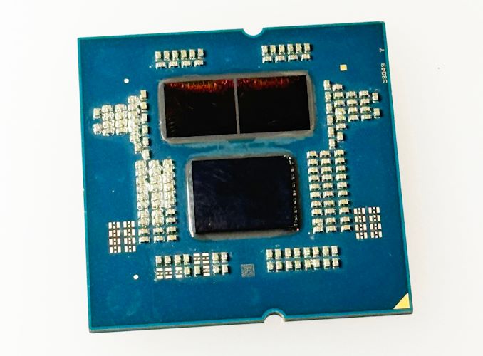
A physical die shot of the AMD Ryzen 9 9950X without the IHS attached
Moving down the Ryzen 9000 stack is the Ryzen 7 9700X, which comes with 8 cores, a max boost clock of up to 5.5 GHz, 32 MB of L3 cache, and a 65W TDP. Finally, the entry-level SKU, the Ryzen 5 9600X, has just 6 cores, a max boost clock of up to 5.4 GHz, 32 MB of L3 cache, and a 65 W TDP.
In terms of design, the Ryzen 9000 with Zen 5 cores and the Ryzen 7000 with Zen 4 cores aren’t too dissimilar; after all, they support the same AM5 motherboards with the LGA1718 CPU socket. At Computex 2024, we confirmed that the Ryzen 9000 series actually uses the same I/O die as the Ryzen 7000 series, which was built using TSMC’s 6 nm process. The only real difference between the Ryzen 9000 and Ryzen 7000 chips is that the Ryzen 9000 incorporates the latest Zen 5 cores in place of Zen 4 cores.
AMD Ryzen 9000 Overclocking: New Curve Shaper Feature
Although the Ryzen 9000 series comes with the Curve Optimizer, which came along with the Zen 3/Ryzen 5000, AMD is introducing a new overclocking feature called Curve

