Future-focused: The trend of miniaturization has consistently fueled technological advancements – from enhancing computing capabilities through smaller transistors to progressing display technologies using micro-LEDs. Researchers from Zhejiang University and the University of Cambridge are now taking LED technology to new heights by introducing the world’s smallest LEDs: nano-PeLEDs, utilizing perovskite semiconductors.
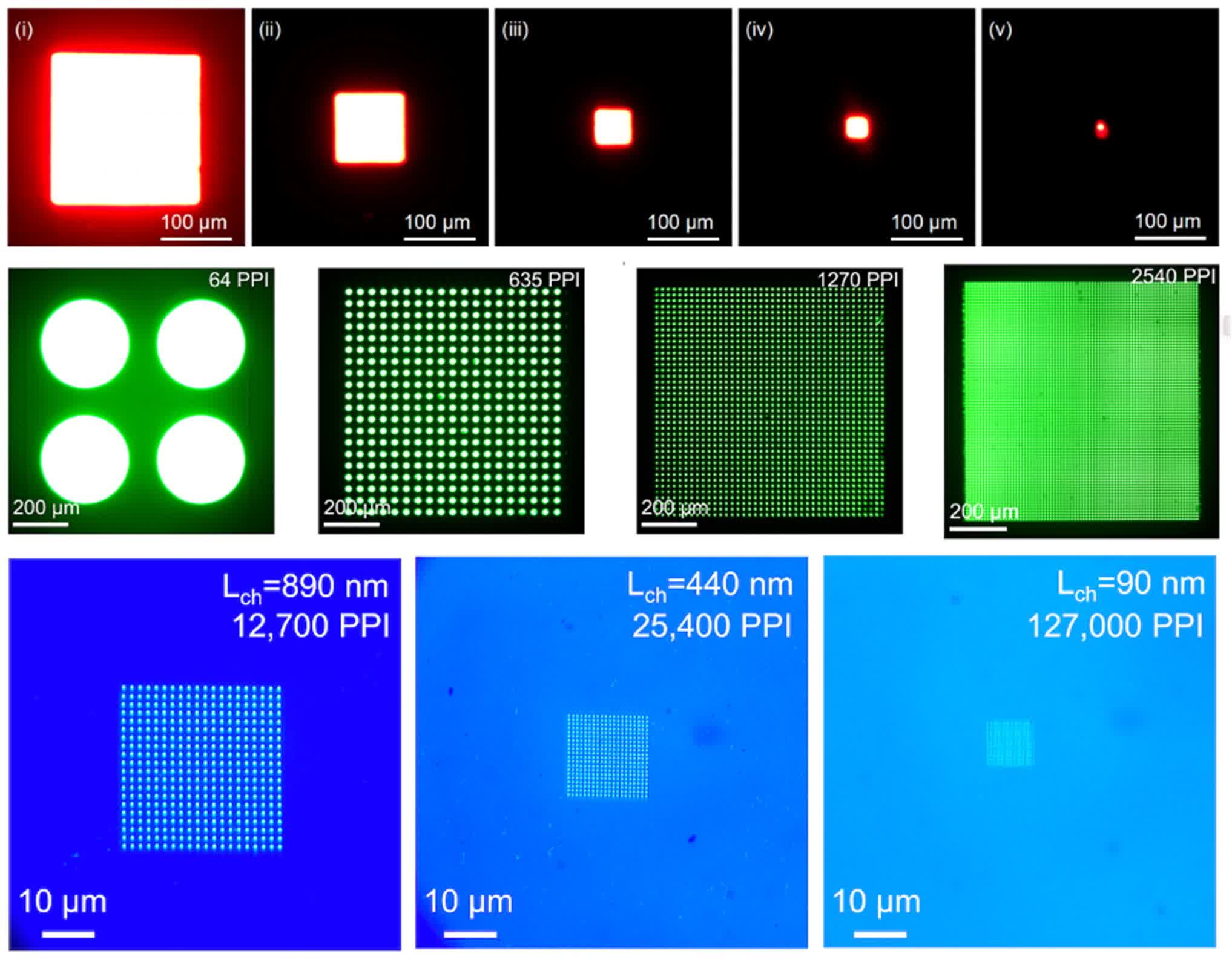
These nano-PeLEDs can achieve pixel lengths as small as 90 nanometers, resulting in an extraordinary pixel density of 127,000 pixels per inch (PPI). In contrast, a standard 27-inch 4K gaming monitor has a pixel density of merely 163 PPI.
“The relentless pursuit to make electronic devices smaller has been a continuous quest for scientists and engineers,” stated Professor Di Dawei, Deputy Director of the International Research Center for Advanced Photonics at Zhejiang University.
He noted that although micro-LEDs constructed from III-V semiconductors are deemed cutting-edge, their efficiency diminishes drastically when pixel sizes drop below 10 micrometers, a limitation that has obstructed their adoption in ultra-high-resolution displays.

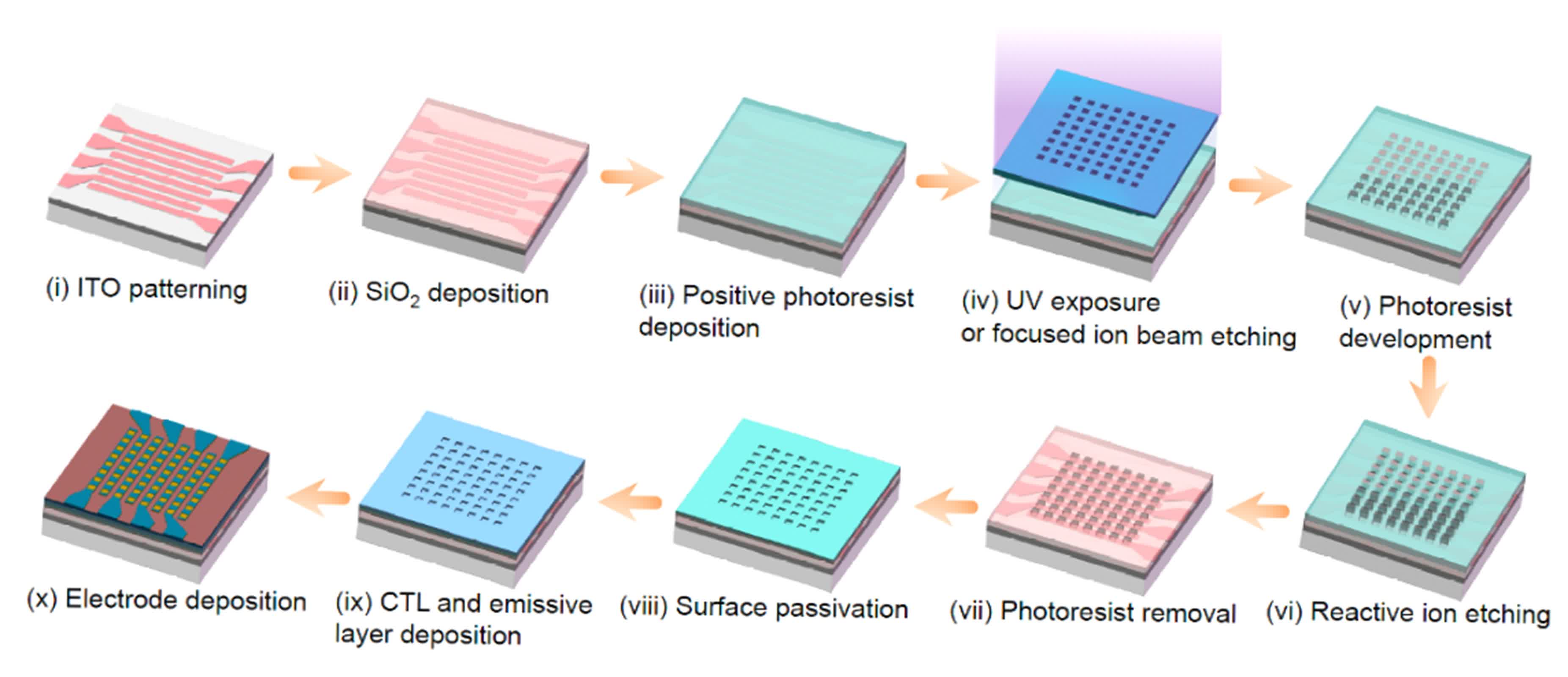
Fabrication techniques for micro- and nano-PeLEDs
In contrast to traditional micro-LEDs, nano-PeLEDs show minimal performance decline even at very small dimensions. This durability is ascribed to their distinct make-up: halide perovskites, a category of semiconductors often linked to solar cells. “Halide perovskites represent a novel family of semiconductors,” stated Professor Zhao Baodan from Zhejiang University.
However, producing nano-PeLEDs is not an easy endeavor. Perovskite materials are notoriously delicate and can be damaged during standard photolithographic techniques used in LED display patterning. To address this issue, the research team devised a groundbreaking fabrication method, utilizing lithographically patterned windows in an insulating layer to safeguard the fragile perovskite material while ensuring high image quality.
“Standard photolithographic techniques are inappropriate for direct patterning of perovskite layers as they would compromise the materials,” remarked Lian Yaxiao, the study’s principal author, whose findings are published in Nature. “Our localized contact fabrication scheme resolves this challenge.”

Red and green micro- and nano-PeLED pixel arrays
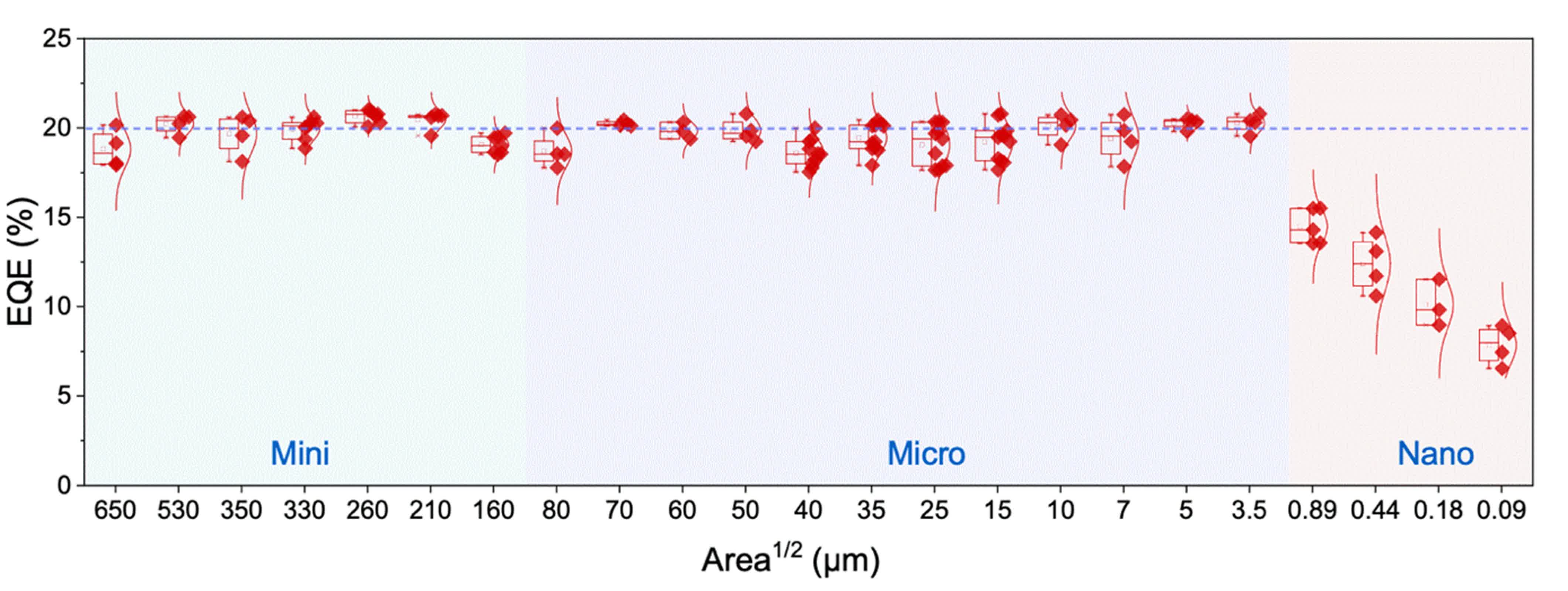
The research team showcased that their green and near-infrared nano-PeLEDs maintained external quantum efficiencies of approximately 20 percent across pixel sizes ranging from several hundred microns down to just 3.5 microns.
Even at extreme miniaturization – about 180 nanometers – the decrease in efficiency was markedly lower than what is observed in classical micro-LEDs. This indicates that nano-PeLEDs may surpass III-V semiconductor-based micro-LEDs in scenarios that demand ultra-small pixel sizes.

Efficiency of micro- and nano-PeLEDs in relation to pixel length
Although nano-PeLEDs present significant potential for high-resolution displays, actual implementation necessitates integration with programmable circuits capable of dynamic content presentation. In this regard, Zhejiang University has joined forces with LinkZill, a Hangzhou-based company that specializes in thin-film transistor (TFT) technology.
Together, they have developed a prototype active-matrix micro-PeLED display powered by a TFT backplane. This prototype is essential for the commercialization of nano-PeLED technology and for realizing its potential for intricate imagery and video playback.

Images from an active-matrix micro-PeLED display
As researchers continue to refine this technology, its potential applications are expanding rapidly. The ultra-high resolution enabled by nano-PeLEDs could transform display standards across multiple sectors – from gaming and augmented reality to medical imaging.


