Why it matters: TSMC’s strategic investments in EUV and high-NA EUV technologies are set to redefine the landscape of semiconductor manufacturing. These significant investments are paving the way for the creation of more potent and efficient chips, applicable across a wide spectrum of uses.
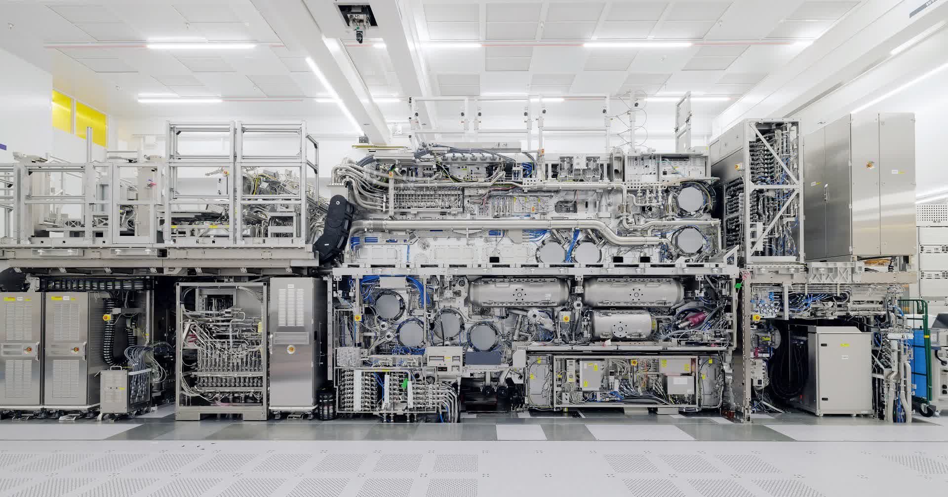
According to Business Korea, TSMC was anticipated to receive its inaugural high numerical aperture (high-NA) extreme ultraviolet (EUV) lithography system, the “EXE:5000,” from the Dutch manufacturer ASML in September 2024. Media coverage diverges on the precise delivery timeline, with some reports indicating installation at TSMC’s Hsinchu R&D facility by year’s end. However, the exact schedule holds less significance compared to the broader implications.
The essential takeaway is TSMC’s evolving position concerning this pioneering technology. Initially adopting a cautious approach, the company has now fully embraced high-NA EUV lithography, ensuring its leadership in the fiercely competitive chip industry where the demand for AI-driven ultra-fine processes is rapidly rising.
Integrating high-NA EUV scanners is crucial for TSMC’s pursuit of sub-2nm processes. These cutting-edge systems enhance the numerical aperture from 0.33 to 0.55, facilitating higher resolution and more precise wafer patterning.
TSMC intends to integrate high-NA EUV scanners into its 1.4nm (A14) process, intended for mass production in 2027.
Nonetheless, these sophisticated lithography systems will not be immediately operational. Extensive testing, fine-tuning, and process optimization will be necessary before their integration into high-volume manufacturing can occur.
By the time these systems become fully operational, TSMC is projected to have progressed to its A10 node, marking several technological advancements beyond its current capabilities. This timeline harmonizes with TSMC’s broader roadmap for advancing chip manufacturing processes.
During TSMC’s Q3 2024 earnings call, CFO Wendell Huang elaborated on the company’s node development schedule. He remarked, “We’re ramping the N2 in 2026. There will also be some preparation costs for ramping N2. As we transition to each leading node, increasingly advanced, these preparation costs will become more substantial.”
Each high-NA EUV system carries a substantial price tag of approximately $384 million. Despite this, TSMC’s pioneering position in high-NA EUV is likely to attract more high-profile customers seeking state-of-the-art chip manufacturing capabilities. This could further extend the gap between TSMC and its competitors, notably Samsung Electronics, which faces challenges in acquiring high-NA EUV equipment.
TSMC has already established a robust foundation with existing EUV technology. The company’s journey with EUV began in earnest in 2019 with the launch of its N7+ process, representing the industry’s first commercial EUV lithography process. Since that time, TSMC has rapidly broadened its EUV capabilities, expanding its EUV systems tenfold between 2019 and 2023.
The ASML team gathers outside their global headquarters in Veldhoven, Netherlands, to celebrate the milestone shipment of the first High-NA EUV lithography system, the TWINSCAN EXE:5000.
The company now commands 56% of the global EUV installation base. The foundry giant has consistently leveraged EUV in subsequent processes, encompassing N5 and N3.
Industry estimates suggest that TSMC operated around 10 EUV systems when it introduced the N7+ process in 2019. In 2022, TSMC acquired 84 EUV systems, and the number exceeded 100 in 2023.
TSMC’s approach to EUV adoption has been methodical and customer-centric. The company carefully assesses new technological innovations based on maturity, cost, and potential customer benefits before incorporating them into mass production. “TSMC plans to bring in high-NA EUV scanners first for R&D to develop the associated infrastructure and patterning solutions needed for customers to fuel innovation,” the company stated to The Register.


